8
Hardware Board Schematics
In This chapter:
- Board Schematics
- Sun-4/470 backplane modifications
- PC Interfaces
- Errata
This chapter contains schematic diagrams of the printed-circuit boards that we designed and built for the DES Cracker. It also includes a few other details about the hardware.
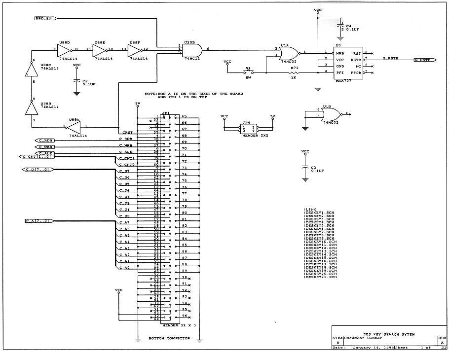
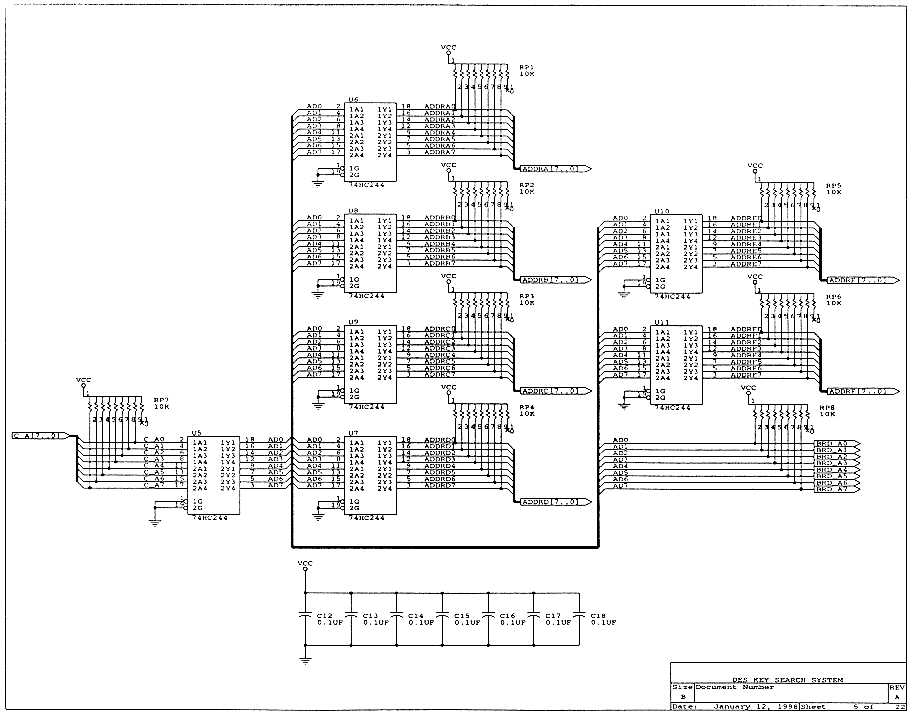
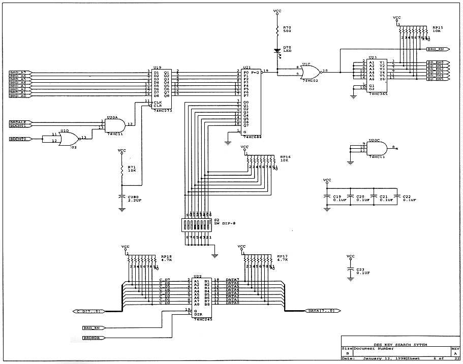
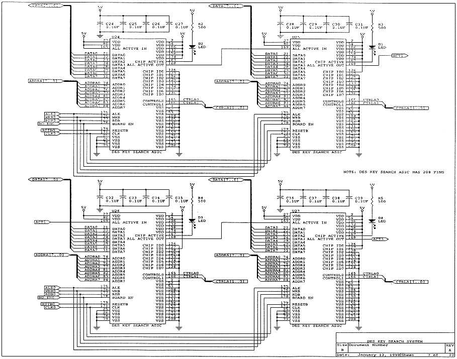
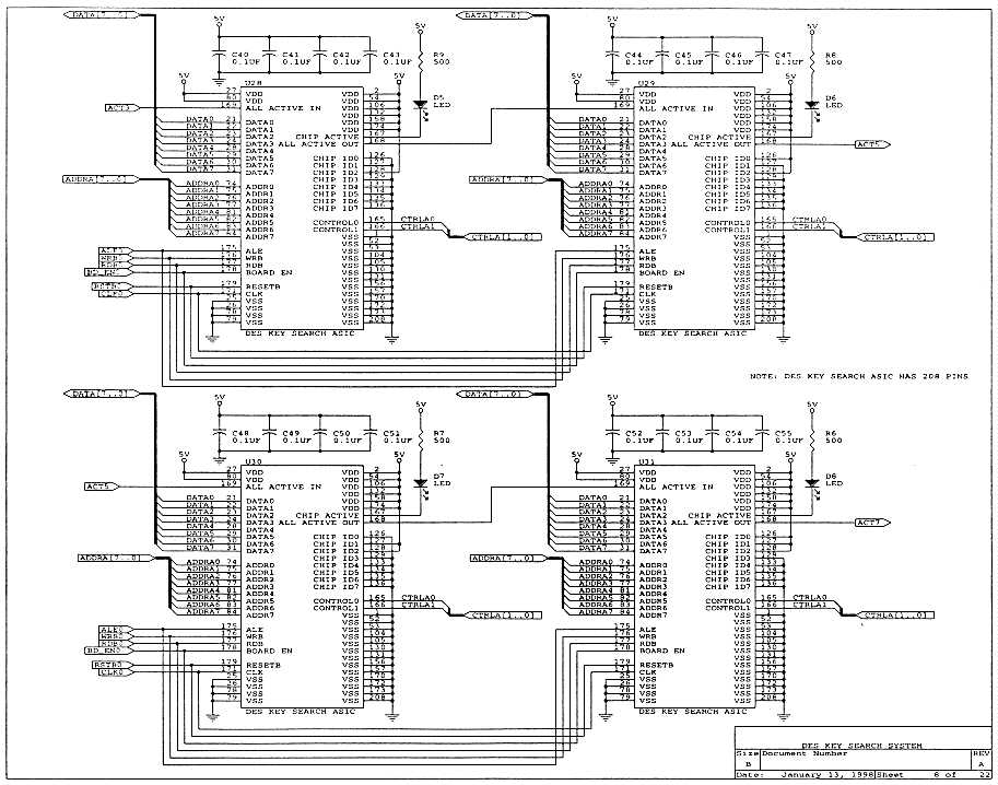
Each hardware board holds 64 DES Cracker chips. In this schematic, we only show how 8 of the chips are wired. The rest are wired almost identically. Each "All Active Out" pin is daisy-chained to the next "All Active In" pin. The "Chip ID" pins on each chip are connected directly to either ground or power, to tell the chip its binary chip number among all the chips on the board. If you examine these pins for the eight chips shown, you'll see how they change.
The boards fit into card-cages which are connected to each other and to the host computer by a 50-pin ribbon cable. The card-cages are modified Sun-4/470 server card cages. The modifications we made to their backplanes are detailed toward the end of the chapter.
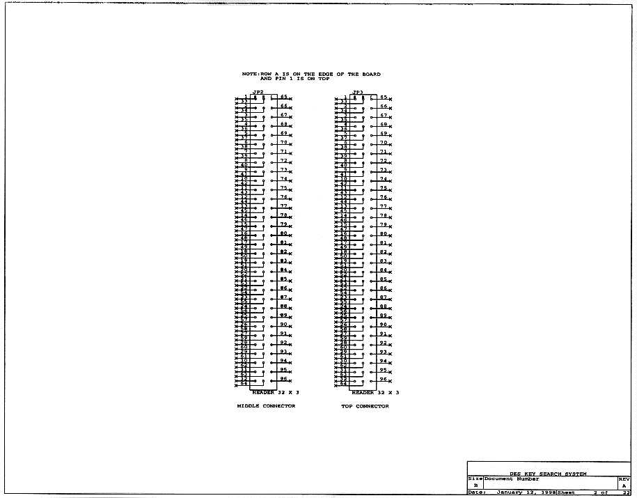
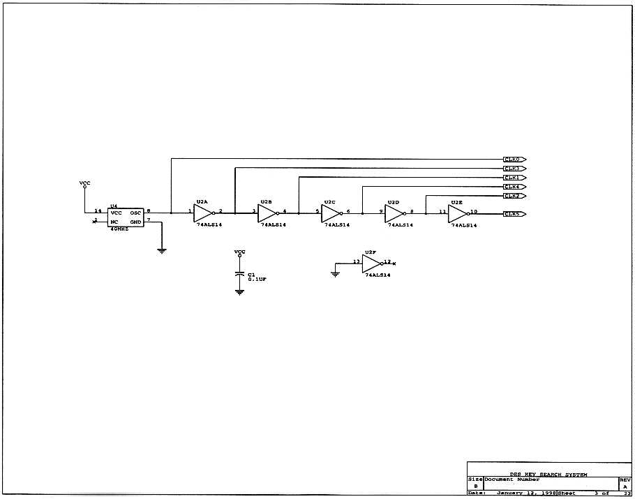
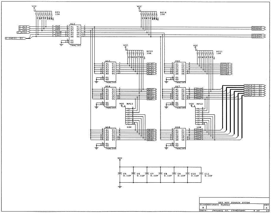
Board Schematics
The schematics begin on the next page. [Note: schematics enlarged 150% to improve readbility.]
8-1
8-2
8-3
8-4
8-5
8-6
8-7
8-8
8-9
8-10
Sun-4/470 backplane modifications
The first DES Cracker uses several chassis recycled from Sun-4/470 servers to hold its boards. Each chassis contains a card cage, power supplies, fans, and covers. In the card cage there is a backplane, which is a printed circuit board that holds the connectors for each board that can be plugged into the card cage. Each row has connectors for 12 slots numbered from 1 to 12. The card cage is sized for "9U" VMEbus boards, each of which has three large 96-pin connectors. Therefore, the backplane also has three 96-pin connectors per board, called P1, P2, and P3. Each of these 96-pin connectors has three rows of 32 pins inside it, called Rows A, B, and C.
We modified the backplane as follows:
Top Row (P1): No modification. We just use this signal from our boards to these connectors.
Middle Row (P2): No modification. We just use this as a board holder. There is no signal from our boards to these connectors.
Bottom Row (P3): Power and signaling for the DES Cracker boards, as follows:
Table 8-1: Signal assignments on bottom connectors |
||
| Row A | Original Assignment | New Assignment |
| Pin 1 to 25 | +5 Volts | Supply voltage for DES Cracker chips |
| Pin 26 to 27 | +12 Volts | Not used |
| Pins 28 to 29 | -12 Volts | Not used |
| Pins 30 to 32 | -5 Volts | Not used |
Row B |
Original Assignment | New Assignment |
| Pin 1 | Reserved | Not used |
| Pin 2 | Reserved | Not used |
| Pin 3 | Reserved | Reset (C_RST) |
| Pin 4 | Reserved | Read Strobe (C_RDB) |
| Pin 5 | Reserved | Write Strobe (C_WRB) |
| Pin 6 | Reserved | Address Latch Enable (C_AEN) |
| Pin 7 | Reserved | Control_1 (C_CNT1) or C_ADRSELB |
| Pin 8 | Reserved | Control_2 (C_CNT2) or C_CSB |
| Pin 9 | Reserved | Data 7 (C_D7) |
| Pin 10 | Reserved | Data 6 (C_D6) |
| Pin 11 | Reserved | Data 5 (C_D5) |
| Pin 12 | Reserved | Data 4 (C_D4) |
| Pin 13 | Reserved | Data 3 (C_D3) |
| Pin 14 | Reserved | Data 2 (C_D2) |
| Pin 15 | Reserved | Data 1 (C_D1) |
8-1
Table 8-1: Signal assignments on bottom connectors (continued) |
||
| Pin 16 | Reserved | Data 0 (C_D0) |
| Pin 17 | Reserved | Address 7 (C_A7) |
| Pin 18 | Reserved | Address 6 (C_A6) |
| Pin 19 | Reserved | Address 5 (C_A5) |
| Pin 20 | Reserved | Address 4 (C_A4) |
| Pin 21 | Reserved | Address 3 (C_A3) |
| Pin 22 | Reserved | Address 2 (C_A2) |
| Pin 23 | Reserved | Reserved Address 1 (C_A1) |
| Pin 24 | Reserved | Address 0 (C_A0) |
| Pin 25 | Reserved | GND |
| Pin 26 | Reserved | GND |
| Pin 27 | Reserved | GND |
| Pin 28 | Reserved | GND |
| Pin 29 | Reserved | GND |
| Pin 30 | Reserved | GND |
| Pin 31 | Reserved | +5 V supply to all Interface ICs |
| Pin 32 | Reserved | +5 V supply to all Interface ICs |
Row C |
Original Assignment | New Assignment |
| Pins 1 to 25 | GND | GND |
| Pins 26 to 27 | +12 Volts | Not used |
| Pins 28 to 29 | -12 Volts | Not used |
| Pins 30 to 32 | -5 Volts | Not used |
Row A, pins 1-25 provide the supply voltage for the DES Cracker chips. The supply is normally +5 Volts.
The chips can be run on a lower voltage, to reduce power consumption and heat generation. In that case, two voltages must be supplied. The lower voltage for the DES Cracker chips is supplied on Row A, pins 1-25. +5 volts is supplied to the interface circuitry on Row B, pins 31 and 32. In low voltage operation, Jumper JP1 on each of the DES boards must be removed. If the DES chips are using +5 Volts, then no external power connects to Row B, pins 31 and 32, and Jumper JP1 on each of the DES boards is connected.
Physical Modifications on P3 Bus (Bottom Row)
The P3 bus (bottom row) of the backplane has 12 slots. Some of these slots are wired to their neighboring slots, forming a bus. In its original Sun configuration, the P3 bus was mainly used for a high-speed memory bus between the CPU board and the memory boards. It was divided into 4 independent groups:
Group 1
This group has 7 slots (from 1 to 7) which have their Row B's bussed together.
8-12
Group 2
This has only slot 8. Its Row B did not connect to any other.
Group 3
This has only slot 9. Its Row B did not connect to any other.
Group 4
This group has 3 slots (from 10 to 12) which have their Row B's bussed together.
We modified the backplane to connect each of these four groups together, so that P3 Row B connects from slot to slot along the whole backplane.
On both slot 1 and slot 12 we added a dual-row header to the P3 connector, Rows B and C (signals and grounds), so that a 50-pin ribbon cable can connect to the bus. These headers allow each chassis to be cabled to the next chassis, and also allow the first chassis to be cabled to a general purpose computer, where the software that controls the DES Cracker runs.
On slot 11, we also added a dual-row header to the P3 connector, Rows A and B (Supply voltage and signals), to let us install termination resistors when no ribbon cable is attached to Slot 12. These protect the integrity of the signals on the bus.
PC Interfaces
The first chassis connects to the controlling computer via a ribbon cable, which attaches to the dual-row header installed on Slot 1. This cable leads to a plug-in hardware card which provides three parallel I/O ports. The software talks to this card, causing it to write commands to the ribbon cable, or read results back from the ribbon cable. The software runs in an ordinary IBM PC, and could be ported to other general purpose computers.
Our project used either of two interface cards. Both are from National Instruments Corporation of Austin, Texas, reachable at http://www.natinst.com or +1 512 794 0100. Their PC-AT bus interface card is called the PC-DIO-24, order number 777368-01. For laptops, a "PC card" (PCMCIA) interface is also available, the DAQCard-DIO-24, order number 776912-01. This card requires the PSH27-SOF-D1 cable, with order number 776989-01.
Other parallel interface cards that provide 24 bit I/O could also be made to work.
8-13
Errata
This page contains notes about errors detected late in the hardware or software published herein.
Chip select for reading
The DES Cracker chips do not properly tristate their data buffers. When any chip on any board is reading, every other DES Cracker chip drives garbage onto its data pins. The buffer enables were not qualified by the Board Enable and Chip Enable signals. The initial hardware boards were modified to circumvent this by providing individual RDB signals to each chip, qualifying them externally with an FPGA. The correct fix is in top.vhd in the chip VHDL; near the last line, change:
DATA <= DATAO when (RDB = '0' and ADDSEL2 = '0') else (others => 'Z'
to:
     DATA <= DATAO when (RDB = '0' and ADDSEL2 = '0' and CHIP_EN = '1')
                   else (others => 'Z');
This also involves adding CHIP_EN as an output of upi.vhd.