In This chapter:
Advanced Wireless Technologies, Inc.
and
Cryptography Research
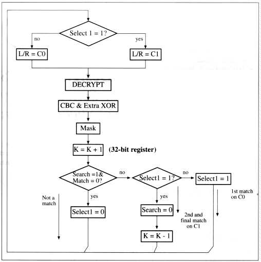
Select1
Selects Cipher text 1
C0
Cipher text 0
C1
Cipher text 1
Search
Search is active
K
Key
Mask
Plain text bit mask and DES output
Match=0
a Zero is found in any bit position of plain text vector as specified in step 4 of Search Unit Operation (see Chapter 2)
CBC & Extra XOR
Perform step 3 of Search Unit Operation (see Chapter 2)
3-1
3-2
Figure 3-1. Search Unit Operation Flow Chart
To determine the maximum number of bit required for the Key:
K= log2(Maximum combinations/number of chips)= log2(256/(24 cpc * 64 cpb * 24 boards) = log2(1. 95E12) = 42 bits
If we are going to use 32-bit counters, then it will overflow every:
232 * 16 cycles * 25ns = 1. 72 * 1012ns = 1720 sec = 28. 7 minutes
3-3
Figure 3-2 State Diagram tor the Search Unit
The PC will interface with the ASICs through a parallel card. The parallel card has three ports, assigned:
Port A: Address(7:0)
Port B: Data(7:0)
Port C: Control, 8 signals
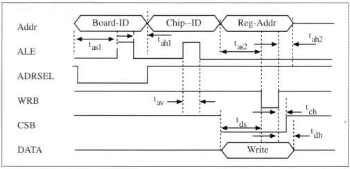
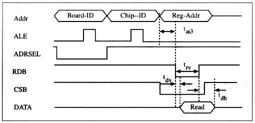
To reduce the routing resources on the boards and ASICs we multiplex the address lines. To access register on the ASIC, it is required that the software latch the
3-4
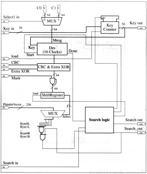
Figure 3-3: Search Unit's Block Diagram
address three times: Board-ID(7:0), Chip-ID(6:0) and then Register address.
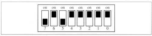
Having switches on the board makes the design flexible and expandable. Each board has its own unique Board-ID configured on switches: for example a board
3-5
with an ID of hexadecimal 5F has its board ID switches configured as follows:
3-6
tas1 10 ns Min Board-ID and Chip-ID Address setup
tas2 10 ns Min Write Register-Address setup
tas3 10 ns Min Read Register-Address setup
tah1 10 ns Min Board-ID and Chip-ID Address invalid (hold)
tah2 10 ns Min Write strobe trailing edge to Address invalid (hold)
tav 10 ns Min ALE valid
tds 10 ns Min Data valid to Write strobe goes low (setup)
tch 10 ns Min Chip select hold
tdh 10 ns Min Write strobe goes high to data invalid (Data hold)
trv 10 ns Min Read strobe duration
tdv 100 ns Max Read strobe goes low to data valid
tdh 100 ns Max Read strobe goes high to data invalid (Data hold)
3-7
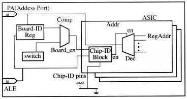
Figure 3-4 Address Bus Scheme
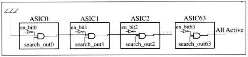
If low the SearchActive bit together. We will place one AND gate per ASIC and cascade them.
3-8
Registers Common to All Search Units |
|
| 0x00-0x1f | PlaintextVector |
| 0x20-0x27 | PlaintextXorMask |
| 0x28-0x2f | CipherText0 |
| 0x30-0x37 | CipherText1 |
| 0x38 | PlaintextByteMask |
| 0x39-0x3e | Reserved |
| 0x3f | SearchInfo |
Additional Registers for Search Units |
|
| 0x40-0x47 | Search Unit 0: Key counter (first 7 bytes) and Search Status |
| 0x48-0x4f | Search Unit 1: Key counter (first 7 bytes) and Search Status |
| . . . | |
| 0xf8-0xff | Search Unit 23: Key counter (first 7 bytes) and Search Status |
Number of register required:
58 common registers + 8 * n registers; n = the total number of search units in an ASIC In this case n = 24, therefore 58 + 192 = 250 registers
3-9
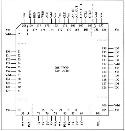
Note: The unspecified pins are Non-Connects
CNTRL0 = ALE = ADDSEL1CNTRL1 = CSB = ADDSEL2